Extensive experience with FPGA/CPLD component selection and software design and verification with a variety of devices from Lattice, Xilinx, Altera, and Cypress Semiconductor. Experience with both integrated and external EEPROM solutions for loading device programming, use of block and distributed RAM, multiple clock domains, and more. Experience using company-provided IP cores and interfacing with dozens of external components, including microcontrollers, EEPROMs, RAM, high-speed ADCs, and more. Hardware design including schematic development and PCB layout of various packages including BGAs.
- Summary
- Experience with small- and medium-sized FPGA, CPLD, and PLD devices
- Experience with Verilog, VHDL, and Abel including mixed VHDL and Verilog designs
- Experience with devices and development environments from a variety of manufacturers
- Experience with maximizing value, reducing BOM cost, and minimizing size by selecting the correct part for the design
- Dozens of designs which include complex operations including implementing state machines, digital filters, closed-loop control systems, forward error correction and parity checks, multiple clock domains, and highly parallel computing
- Interfaces with external logic analyzers for development and test
- Use of in-system debug tools for access to real-time internal logic to replace logic analyzer connections
- Use of simulators and HDL codes synthesizers using MATLAB and Simulink
- Hardware
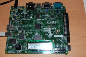
- Xilinx Spartan-3E FPGA
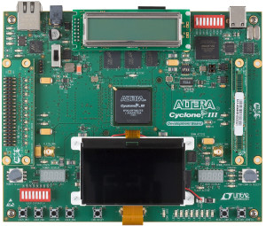
- Altera Cyclone III FPGA
- Lattice MachXO CPLD/FPGA Crossover
- More than ten other smaller devices
- Languages
- Verilog, VHDL, and Abel
- Mixed Verilog/VHDL designs
- C and C++ in a NiOS Softcore Processor
- MATLAB and Simulink generation of both VHDL and Verilog
- Xilinx and Lattice IP Cores (FIFO and LIFO stacks, DDR SDRAM memory interface, synchronous memory interface, UART, and SPI) for code generation
- Development Environments
- Lattice ispLEVER
- Xilinx ISE Design Suite
- Altera Quartus II
- Use of Integrated Features
- Block and distributed RAM
- Differential and singled-ended signalling
- Pull-up/pull-down resistors and open collector outputs
- Integrated multipliers including pipelines
- Digital Clock Managers (DCM) including frequency synthesis, multiplication, division, and phase shifting
- Use of both external and integrated EEPROM for image loading
- Use of devices that include integrated DC-DC power supply for core voltage generation and devices that require separate external power supplies with multiple voltages (typically 1.2 V, 2.5 V, and 3.3 V)
- Interface Devices
- 8- and 12-bit high-speed ADCs for radio receiver interaction
- RF switches for transmitters
- PFETs and comparators for uninterrupted power source selection
- PSRAM for volume data buffering
- Microcontrollers and other processors, typically via high-speed parallel connections
- Project Highlights
- Experience interfacing FPGA/CPLD with microcontrollers, high-speed (80 MSPS) ADCs for both superhet and direct conversion receivers involving log RF power detectors and IQ demodulation
- Using FPGA for power source selection circuit (selecting between battery, generator, and shore power)
- Implementing decoding techniques using cyclic codes for both error detection and correction (forward error correction)
- Advanced techniques for detecting magnitude and phase when interfacing with IQ demodulator (with high-speed ADC)
- Experience with implementing closed-loop feedback systems, including digital low-, band-, and high-pass filters